What’s is that about?
SoC stands for System on Chips. If you want to have fun with a technology soupe, SoCs are for you. Think about it: you get a board with a two ARM processors running a Linux kernel surrounded by an FPGA. If you followed the SDK from Terasic – which are very good starting point BTW –, the FPGA has to be programmed from VHDL/Verilog – more about that later –, the integration with the FPGA is done via Altera QSys IP designer, the processors are running a Linux armhf program written in C. That already looks complex but not quite enough.
I’m not very much attracted by Verilog/VHDL languages but much more interested by higher level languages that compile into that. Have already played a bit with Kansas Lava but this time will give a shot to Clash. As for the program running on the ARM, C is … from another age. Let’s use Golang.
The purpose of this post is not to make a rocket autopilot, just to demonstrate how to use this platform, provide a few hints one how to get those things working together and maybe inspire you to make your a rocker autopilot. For those in the area, San Mateo Makerfaire is in few weeks.
The board I’m using here is a relatively inexpensive board from Terasic named – not without some form of peotry: DE0-Nano-SoC.
Setup
If you have the board, a laptop with a linux or windows (where you can run Altera Quartus) and the board you are good to go. I’m using version 15.1 of Quartus in a Windows vm as my dev machine is a Mac.
The board is attached via 2 USB cables: one for the serial programmer, one for the console. To use the serial programmer, you need to set the dip switch on the upper-left corner of the board to 101011. I have also plugged the ethernet cable to my network so I can transfer the program using SCP – first use the console to set the interface up, root password and get the IP. Alternatively if you have a micro-SD adaptor, you can copy the Linux program directly on the sdcard with the OS.
Then you’ll need Quartus which you can download from Altera’s website. Quartus comes with Qsys which will let you defines how the processor is connected to the memory, and more generally the FPGA and its I/O.
Finally, Clash will be used to generate the logic on the FPGA side.
Goal
The goal is more to get acquainted with the platform and device rather than do anything usefull. And also since the goal is not to get lost in the way, I have basically copied one of the Terasic SDK projects. This projects uses the FPGA to expose the LEDs and the switches of the board to the processors space and use a small program to update the LEDs according to the states of the switches. You’ll be able to find the original project on Terasic resources page for the DE0-Nano-SoC. To make that a bit more complicated and also because I wanted to play with Clash, we will add a module written in Clash in the chain between the switches and the LEDs.
So the theory of the operations is as follow: - the state of the switches is passed to a module written in Clash - the output of this module is fed connected to the bus which is attached to the processors - from the userland part of the Linux running on the processors, a go program will read the value and write it to something that is conncted to the LEDs via another IO interface on the bus. - finally the switches, and LEDs IO pins are mapped from the SoC to the right pin of the board.
Let’s details these elements a bit more in the next section.
Blocks
This project uses the Lightweight HPS-to-FPGA AXI bridge. If you wonder what this thing is, think of an memory-mapped access to the FPGA1. For those who have played with QSys and NIOSII processors with its avalon bus, Qsys edition for SoC integrates the HPS and its bus very smoothly and is able to bridge Avalon2 peripherics to it.
So essentilly what we end up with on our bus is:
- a clock source
- the HPS,
- 2 PIOs3: one for the switches, one for the LEDs
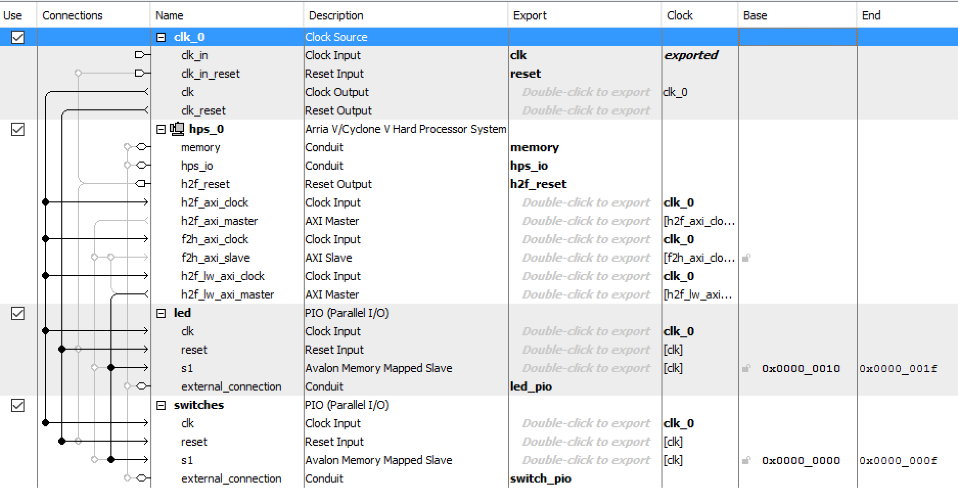
Note the exported signals as well as the address of the two PIOs. They will be useful to connect and use this design.
These PIOs speak the language of the bus on one side and provide a parallel interface on the other which we will interface with the LEDs and the switches. As you’ll have understood, they will be condifured in the opposite directions.
On the other side of the bus, we will connect the LEDs and switches bus that the project generator from Terasic will have generated for us – Which is essentially a mapping of the FPGA’s pin to IOs of the top-level HDL entity4.
Now let’s have a quick look at the logic we add on the FPGA. Since this project is just about showing what can be done, the logic will be pretty simple and just square a 4bit signal. This module will be plugged between the switches and the switch PIOs.
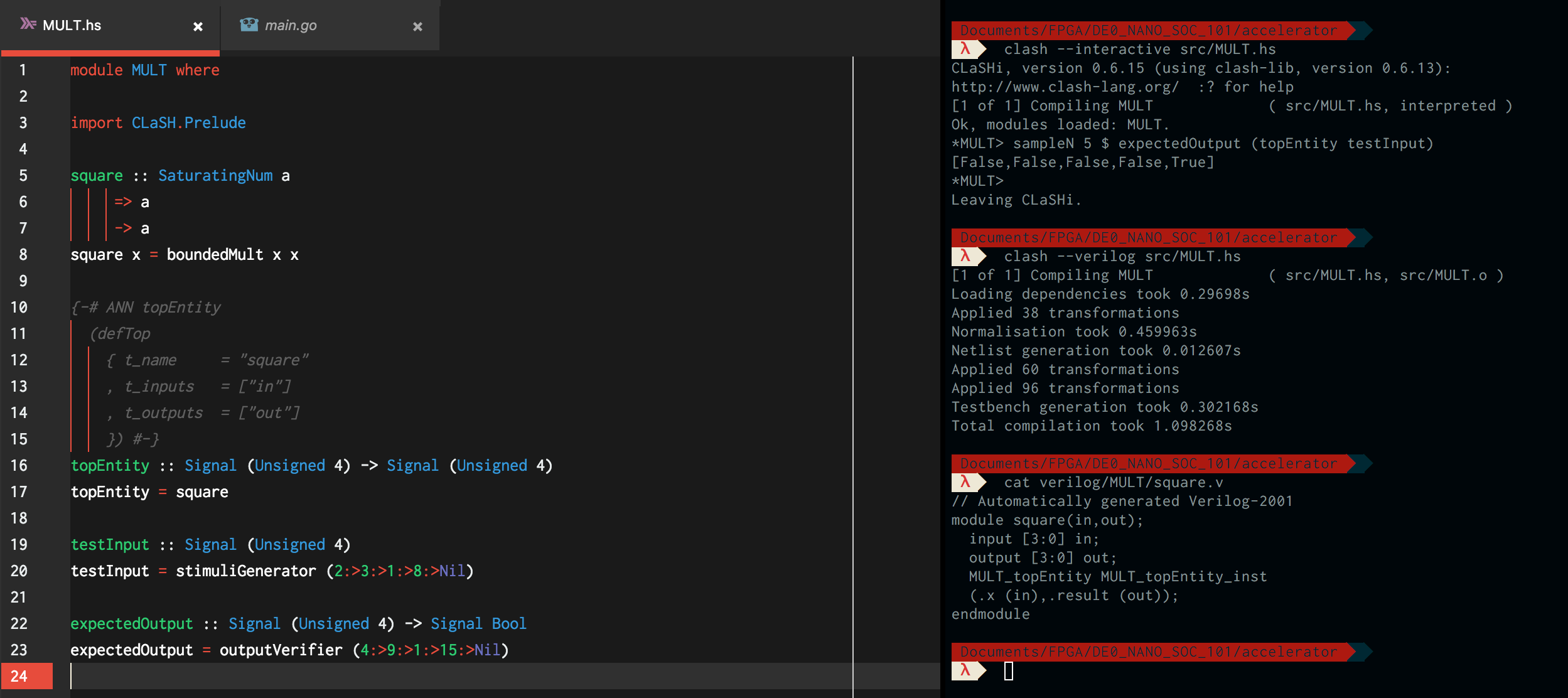
As you can see, nothing too elite, but a simple setup to test communications in each direction, and interfacing with the external world.
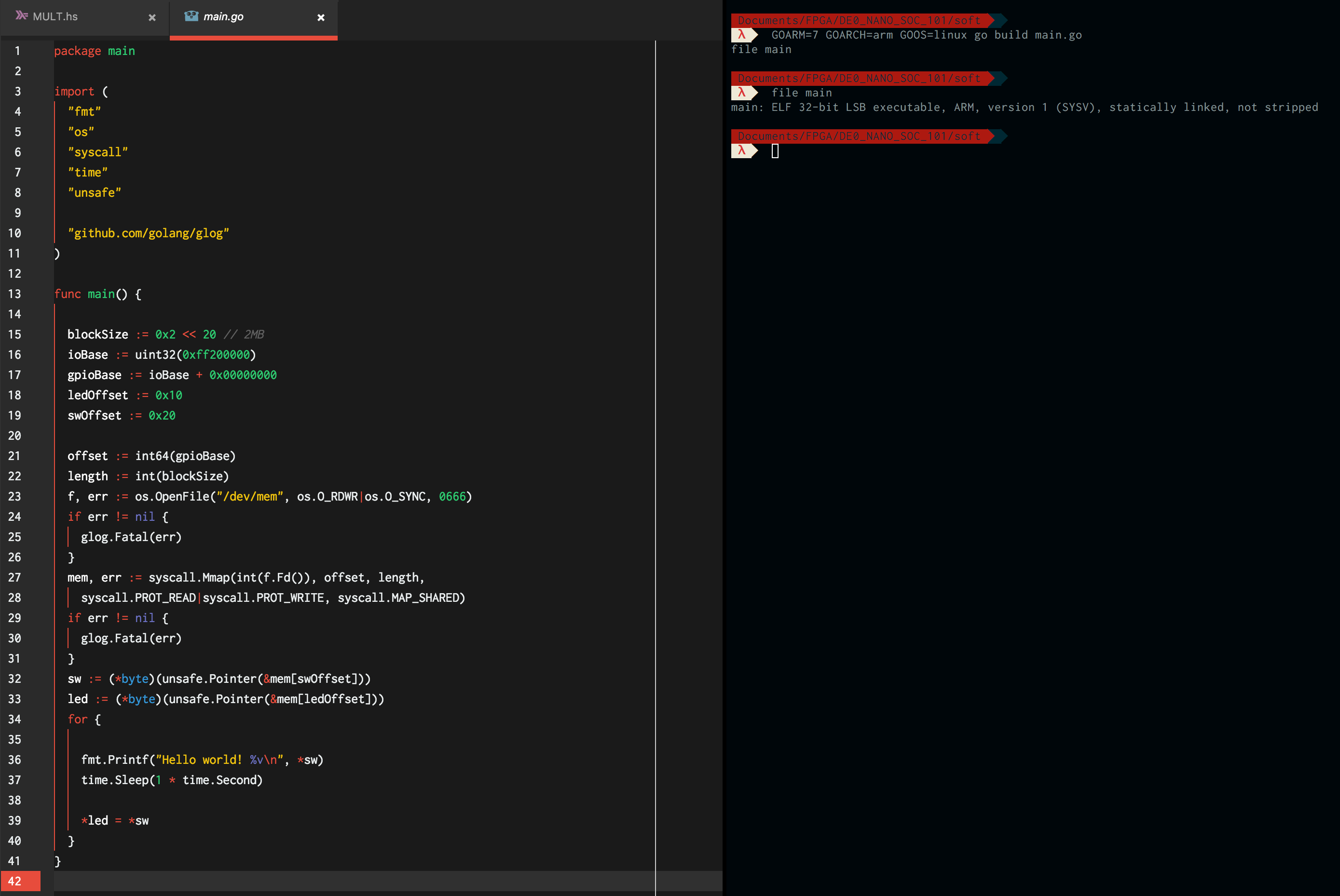
Then, the last piece is the software that will run on the HPS. We have used memory mapped peripherics, we will use /dev/mem to access them. Note that during the setup of the PIOs we can choose the address and thanks to the documentation we know the base address which is used from the HPS side to access these, we can easily compute the address we want to read/write.
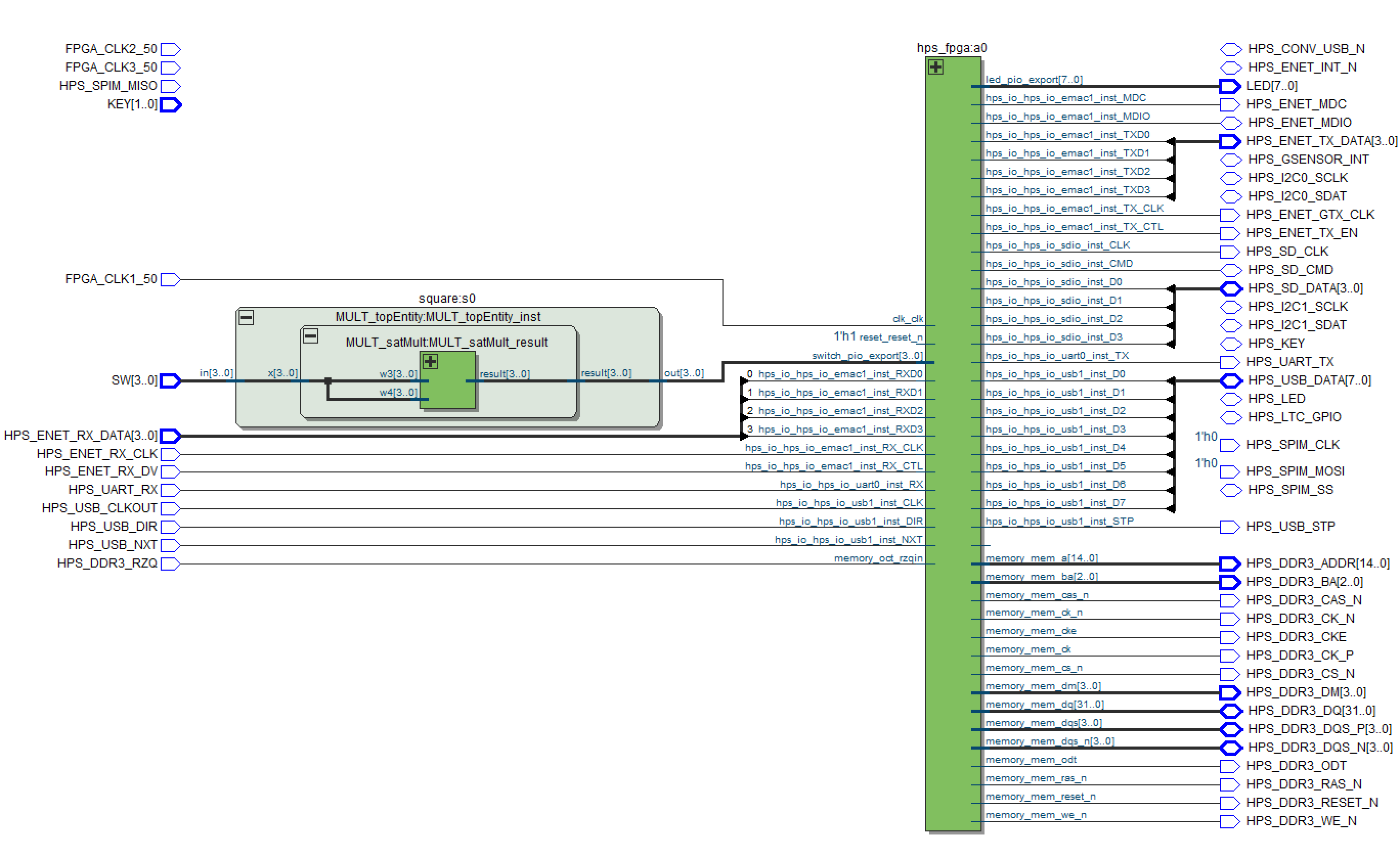
After copying, and integrating the verilog taht clash has generated for us with the code Qsys has generated on his side into the top-level entity of the Quartus project, the circuit on the FPGA looks as follow:
A bit of place&route, programming file generation, FPGA programming via USB-blaster, go program cross-compilation, copy over SCP to the board… later, we can run the program and play with the switches to turn on and off the LEDs.
Take away
- Don’t name your QSys design ‘hps’. It creates conflicts.
- Look at this video5 for the detailed setup of the bridge. Though it is for DE1 board, with minor adaptations it works fine for DE0.
- Pins to DRAM memory are not configured and need to be configued with the ‘pin editor’ to add all kind of constraints (delay compensation, current, input and output impedence). For that I recommend you to look at one of the example from Terasic, that’s where I have copied the values from.
- With the dip switch configuration defined earlier, you can use the USB blaster to configure the FPGA6.
- the HPS is an ARM7 so
GOARM=7 GOARCH=arm GOOS=linux go build main.goand you are good to… - Terasic SDKs and manuals are very helpful to setup a first project.
- Clash is a very intersting alternative to write HDL (verilog/vhdl). Check this project out: HaSKI.
Show me the code!
Here is the code for this project. There isn’t much of it. First is the component written in Clash which square the 4bit signal, second is the code which read the memory-mapped switches and write them to the LEDs registers. Note that since the ‘square’ component is between the switches and the HPS block, what is actually read by the program in Go is the squared signal and not the state of the switches.
module MULT where

import CLaSH.Prelude

square :: SaturatingNum a
     => a
     -> a
square x = boundedMult x x

{-# ANN topEntity
  (defTop
    { t_name     = "square"
    , t_inputs   = ["in"]
    , t_outputs  = ["out"]
    }) #-}
topEntity :: Signal (Unsigned 4) -> Signal (Unsigned 4)
topEntity = square

testInput :: Signal (Unsigned 4)
testInput = stimuliGenerator (2:>3:>1:>8:>Nil)

expectedOutput :: Signal (Unsigned 4) -> Signal Bool
expectedOutput = outputVerifier (4:>9:>1:>15:>Nil)
Clash uses some special comments (annotation) to define the naming of the entities and I/Os in the generated HDL.
The top-level entity of our Quartus project is as follow:
module accelerator_soc(

	//////////// CLOCK //////////
	input 		          		FPGA_CLK1_50,
	input 		          		FPGA_CLK2_50,
	input 		          		FPGA_CLK3_50,

	//////////// HPS //////////
	inout 		          		HPS_CONV_USB_N,
	output		    [14:0]		HPS_DDR3_ADDR,
	output		     [2:0]		HPS_DDR3_BA,
	output		          		HPS_DDR3_CAS_N,
	output		          		HPS_DDR3_CK_N,
	output		          		HPS_DDR3_CK_P,
	output		          		HPS_DDR3_CKE,
	output		          		HPS_DDR3_CS_N,
	output		     [3:0]		HPS_DDR3_DM,
	inout 		    [31:0]		HPS_DDR3_DQ,
	inout 		     [3:0]		HPS_DDR3_DQS_N,
	inout 		     [3:0]		HPS_DDR3_DQS_P,
	output		          		HPS_DDR3_ODT,
	output		          		HPS_DDR3_RAS_N,
	output		          		HPS_DDR3_RESET_N,
	input 		          		HPS_DDR3_RZQ,
	output		          		HPS_DDR3_WE_N,
	output		          		HPS_ENET_GTX_CLK,
	inout 		          		HPS_ENET_INT_N,
	output		          		HPS_ENET_MDC,
	inout 		          		HPS_ENET_MDIO,
	input 		          		HPS_ENET_RX_CLK,
	input 		     [3:0]		HPS_ENET_RX_DATA,
	input 		          		HPS_ENET_RX_DV,
	output		     [3:0]		HPS_ENET_TX_DATA,
	output		          		HPS_ENET_TX_EN,
	inout 		          		HPS_GSENSOR_INT,
	inout 		          		HPS_I2C0_SCLK,
	inout 		          		HPS_I2C0_SDAT,
	inout 		          		HPS_I2C1_SCLK,
	inout 		          		HPS_I2C1_SDAT,
	inout 		          		HPS_KEY,
	inout 		          		HPS_LED,
	inout 		          		HPS_LTC_GPIO,
	output		          		HPS_SD_CLK,
	inout 		          		HPS_SD_CMD,
	inout 		     [3:0]		HPS_SD_DATA,
	output		          		HPS_SPIM_CLK,
	input 		          		HPS_SPIM_MISO,
	output		          		HPS_SPIM_MOSI,
	inout 		          		HPS_SPIM_SS,
	input 		          		HPS_UART_RX,
	output		          		HPS_UART_TX,
	input 		          		HPS_USB_CLKOUT,
	inout 		     [7:0]		HPS_USB_DATA,
	input 		          		HPS_USB_DIR,
	input 		          		HPS_USB_NXT,
	output		          		HPS_USB_STP,

	//////////// KEY //////////
	input 		     [1:0]		KEY,

	//////////// LED //////////
	output		     [7:0]		LED,

	//////////// SW //////////
	input 		     [3:0]		SW
);


//=======================================================
//  REG/WIRE declarations
//=======================================================
wire hps_fpga_reset_n;
wire [7:0] led_pio;
wire [3:0] switch_pio;

//=======================================================
//  Structural coding
//=======================================================

assign LED = led_pio;

// Instanciation of our squaring entity
square s0(SW, switch_pio);

// Instanciation of the QSys-generated design
hps_fpga a0 (
    //
    .clk_clk(FPGA_CLK1_50),
    .reset_reset_n(1'b1),
    //
    .h2f_reset_reset_n(hps_fpga_reset_n),
    // HPS ethernet
    .hps_io_hps_io_emac1_inst_TX_CLK ( HPS_ENET_GTX_CLK),
    .hps_io_hps_io_emac1_inst_TXD0   ( HPS_ENET_TX_DATA[0] ),
    .hps_io_hps_io_emac1_inst_TXD1   ( HPS_ENET_TX_DATA[1] ),
    .hps_io_hps_io_emac1_inst_TXD2   ( HPS_ENET_TX_DATA[2] ),
    .hps_io_hps_io_emac1_inst_TXD3   ( HPS_ENET_TX_DATA[3] ),
    .hps_io_hps_io_emac1_inst_RXD0   ( HPS_ENET_RX_DATA[0] ),
    .hps_io_hps_io_emac1_inst_MDIO   ( HPS_ENET_MDIO ),
    .hps_io_hps_io_emac1_inst_MDC    ( HPS_ENET_MDC  ),
    .hps_io_hps_io_emac1_inst_RX_CTL ( HPS_ENET_RX_DV),
    .hps_io_hps_io_emac1_inst_TX_CTL ( HPS_ENET_TX_EN),
    .hps_io_hps_io_emac1_inst_RX_CLK ( HPS_ENET_RX_CLK),
    .hps_io_hps_io_emac1_inst_RXD1   ( HPS_ENET_RX_DATA[1] ),
    .hps_io_hps_io_emac1_inst_RXD2   ( HPS_ENET_RX_DATA[2] ),
    .hps_io_hps_io_emac1_inst_RXD3   ( HPS_ENET_RX_DATA[3] ),
    // HPS SD card
    .hps_io_hps_io_sdio_inst_CMD     ( HPS_SD_CMD    ),
    .hps_io_hps_io_sdio_inst_D0      ( HPS_SD_DATA[0]     ),
    .hps_io_hps_io_sdio_inst_D1      ( HPS_SD_DATA[1]     ),
    .hps_io_hps_io_sdio_inst_CLK     ( HPS_SD_CLK   ),
    .hps_io_hps_io_sdio_inst_D2      ( HPS_SD_DATA[2]     ),
    .hps_io_hps_io_sdio_inst_D3      ( HPS_SD_DATA[3]     ),
    // HPS USB
    .hps_io_hps_io_usb1_inst_D0      ( HPS_USB_DATA[0]    ),
    .hps_io_hps_io_usb1_inst_D1      ( HPS_USB_DATA[1]    ),
    .hps_io_hps_io_usb1_inst_D2      ( HPS_USB_DATA[2]    ),
    .hps_io_hps_io_usb1_inst_D3      ( HPS_USB_DATA[3]    ),
    .hps_io_hps_io_usb1_inst_D4      ( HPS_USB_DATA[4]    ),
    .hps_io_hps_io_usb1_inst_D5      ( HPS_USB_DATA[5]    ),
    .hps_io_hps_io_usb1_inst_D6      ( HPS_USB_DATA[6]    ),
    .hps_io_hps_io_usb1_inst_D7      ( HPS_USB_DATA[7]    ),
    .hps_io_hps_io_usb1_inst_CLK     ( HPS_USB_CLKOUT    ),
    .hps_io_hps_io_usb1_inst_STP     ( HPS_USB_STP    ),
    .hps_io_hps_io_usb1_inst_DIR     ( HPS_USB_DIR    ),
    .hps_io_hps_io_usb1_inst_NXT     ( HPS_USB_NXT    ),
    // HPS UART
    .hps_io_hps_io_uart0_inst_RX     ( HPS_UART_RX   ),
    .hps_io_hps_io_uart0_inst_TX     ( HPS_UART_TX   ),
    // LED PIO
    .led_pio_export                  ( led_pio ),
    // HPS ddr3
    .memory_mem_a                          ( HPS_DDR3_ADDR),
    .memory_mem_ba                         ( HPS_DDR3_BA),
    .memory_mem_ck                         ( HPS_DDR3_CK_P),
    .memory_mem_ck_n                       ( HPS_DDR3_CK_N),
    .memory_mem_cke                        ( HPS_DDR3_CKE),
    .memory_mem_cs_n                       ( HPS_DDR3_CS_N),
    .memory_mem_ras_n                      ( HPS_DDR3_RAS_N),
    .memory_mem_cas_n                      ( HPS_DDR3_CAS_N),
    .memory_mem_we_n                       ( HPS_DDR3_WE_N),
    .memory_mem_reset_n                    ( HPS_DDR3_RESET_N),
    .memory_mem_dq                         ( HPS_DDR3_DQ),
    .memory_mem_dqs                        ( HPS_DDR3_DQS_P),
    .memory_mem_dqs_n                      ( HPS_DDR3_DQS_N),
    .memory_mem_odt                        ( HPS_DDR3_ODT),
    .memory_mem_dm                         ( HPS_DDR3_DM),
    .memory_oct_rzqin                      ( HPS_DDR3_RZQ),
    .switch_pio_export                     ( switch_pio ),
    );


endmodule
We can not the instanciation of the two entities: hps_fpga and square and how they are connected to switches (SW input signal) and LEDs (LED output signal).
Now on the software side, the Go program is simply opening /dev/mem at the right address (base address provided in the user manual of the board) and reading/writting memory from here at the offset we have defined in Quartus:
package main

import (
	"fmt"
	"os"
	"syscall"
	"time"
	"unsafe"

	"github.com/golang/glog"
)

func main() {

	blockSize := 0x2 << 20 // 2MB
	ioBase := uint32(0xff200000)
	gpioBase := ioBase + 0x00000000
	ledOffset := 0x10
	swOffset := 0x20

	offset := int64(gpioBase)
	length := int(blockSize)
	f, err := os.OpenFile("/dev/mem", os.O_RDWR|os.O_SYNC, 0666)
	if err != nil {
		glog.Fatal(err)
	}
	mem, err := syscall.Mmap(int(f.Fd()), offset, length,
		syscall.PROT_READ|syscall.PROT_WRITE, syscall.MAP_SHARED)
	if err != nil {
		glog.Fatal(err)
	}
	sw := (*byte)(unsafe.Pointer(&mem[swOffset]))
	led := (*byte)(unsafe.Pointer(&mem[ledOffset]))
	for {

		fmt.Printf("Hello world! %v\n", *sw)
		time.Sleep(1 * time.Second)

    // Copy the input to the output
		*led = *sw
	}
}
Next step
And that’s how ends what was initially a weekend project7. Two things to explore next: what are the other way to interface the processors with the FPGA and how usefull could that be to make some computations in the FPGA?
AXI is an interface of AMBA, the ‘PCI bus’ for ARM processors.↩︎
Another inter-connect…↩︎
Parallel IO interfaces↩︎
Plus probably some configuration of the pins themselves as we will see later.↩︎
Thanks man! very helpful.↩︎
But it looks fun to do that from the Linux itself via
/dev/fpga0, for that check the DE0 user manual which details how to generate the parallel programming file and which dip configuration to use.↩︎I know I should not put that many footnotes.↩︎
